Why the photon computer did not work for 30 years
In 1990, Demetri Psaltis, a professor of optoelectronics at Caltech, published inNaturean article that was supposed to change the face of computer science. He showed that a hologram could perform neural network calculations — not with transistors, but with light. The electrons are free, they heat up the system and lose energy into resistance. Light has none of these problems.
Thirty-five years later, NVIDIA graphics cards are powering the entire AI revolution, and photonic computers still sit on lab benches - demonstrative, flashy, and useless outside of a controlled environment.
Why?
The answer does not lie in physics. The physics worked from day one. The problem was purely engineering and had exactly three layers. To understand why none of them have given up for three decades, you have to go back to the moment when scientists first believed they could be defeated.
First wall: crosstalk
In 2017, Yichen Shen's team at MIT published wNature Photonicsbreakthrough work: They built a nanophotonic chip that performed matrix multiplication - the fundamental operation of any neural network - using only light. The system worked. The problem was that it had only 56 optical components.
To compete with silicon electronics, a photonic accelerator would have to have thousands of them. Each additional element – modulator, splitter, coupler – introduced its own thermal noise, degraded the signal-to-noise ratio, and generated crosstalk between adjacent waveguide channels. Engineers tried to scale. It worked for several hundred elements. Then the circuit became unusable - the output signal looked more like a coin toss than the result of matrix multiplication.
Shen and his colleagues tried adaptive calibration, an algorithm that would correct each modulator's thermal drift in real time. It worked with 56 items. At 200 - the algorithm couldn't keep up.
The second wall: a memory that is gone
The electron can be retained. A transistor is nothing more than a controlled trap for electric charge - you hold it in and release it when you need it. A photon cannot be stopped in a similar way. Yes, there are optical resonators that can trap light for several dozen picoseconds - but this is not enough to build memory.
The consequence is brutal: a photonic accelerator must constantly convert signals between the optical and electronic domains to perform a meaningful calculation. Light performs the multiplication - electronics stores the result. Light receives new data - electronics formats it. Each light-electron-light conversion costs exactly what photonic computers were designed to eliminate: time.
Teams from Oxford, Princeton, and MIT tried various workarounds. All-optical systems - no conversion, pure photonics. Nonlinear optical activations instead of electronic ones. The problem is that nonlinearity in photonics requires either extremely high optical powers (on the order of watts per waveguide - the chip would melt) or exotic materials that are not suitable for mass production.
Third wall: the algorithm looks for hardware, the hardware looks for the algorithm
The year is 2020. Charles Roques-Carmes, a PhD student at Stanford, is publishing inNature Communicationsa heuristic algorithm specially designed for photonic Ising machines - systems that solve difficult optimization problems by physically simulating spin networks. The algorithm is elegant. The problem is that Roques-Carmes tests it on a simulator. There is simply no physical system of sufficient scale.
This is where the three walls form a perfect loop: you can't scale a system without a mature manufacturing process. It is not profitable to build a production process without proving that the system at scale works. You can't prove it works without an algorithm - and no one will write an algorithm unless you have the equipment to test it.
For thirty years, the industry has circled this triangle.
16,000 components and the third dimension
In April 2025, the same Roques-Carmes - already as a co-author - signed the article inNature, which breaks the loop. Together with a 25-person team from Lightelligence, a Singaporean startup founded by Yichen Shen, they presented the PACE system: a photonic accelerator containingover 16 thousand optical componentson a single chip.
That's more than all previous demonstrators combined.
The key to breaking the first wall did not lie in new physics. It lay in what looks like packaging engineering from the outside, but is actually a fundamental architectural breakthrough:2.5D hybrid advanced packaging
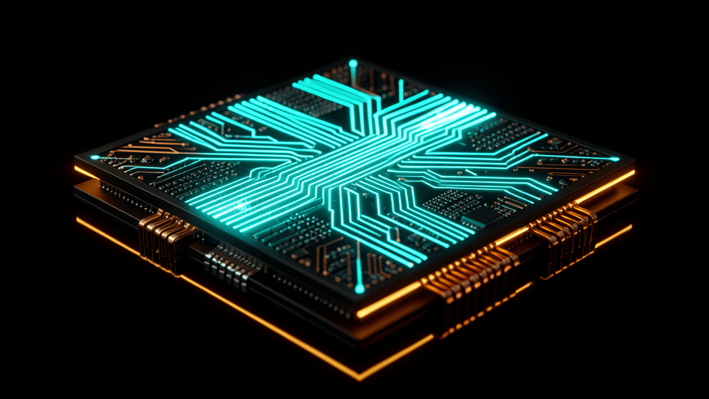
Imagine a three-story building. On the ground floor - electronics: ARM processor, memory controllers, analog-to-digital converters, control logic. On the first floor - a dense matrix of copper micro-connections, spaced every few dozen micrometers. On the second floor - a photonic chip with 16,000 waveguides, modulators and photodetectors. Communication between floors does not take place through single connections at the edges (as in a traditional multi-chip module), but through thousands of vertical channels distributed evenly over the entire surface.
The result: crosstalk between channels drops dramatically because each optical channel has its own, isolated electronic path. Thermal noise can be corrected selectively - the calibration algorithm no longer has to track all 16,000 components at once, but manages clusters of 64 components.
The architecture also allows for a partial solution to the memory problem. Instead of converting each individual optical result back to the electronics, PACE buffers them in the analog domain right at the chip boundary - minimizing the number of conversions.
Result? The system performs 64×64 matrix multiplication at a clock frequency1 GHz. Single calculation cycle:3 nanoseconds. For comparison, the NVIDIA A10 GPU, Ampere architecture from 2021, needs hundreds of nanoseconds for the same task, even with optimal scheduling of operations in the systolic array structure.
In the practical test - solving Ising problems, i.e. finding the spin configuration that minimizes energy in a network with interactions (the same type of mathematics as optimizing courier routes, scheduling production or allocating resources in data centers) - PACE wastwo to three times fasterthan A10. Not thanks to higher throughput - thanks to two orders of magnitude lower latency per single iteration step.
NVIDIA A10 performs a huge number of operations in parallel, but each iteration of the algorithm requires data to be transferred between the cores and then from GPU memory back to the computing units. PACE performs fewer operations at a time, but the results are available immediately.
Who invests
Lightelligence has raised over200 million dollarsfrom investors including Baidu Ventures and Singapore's sovereign fund Temasek. The company employs over 150 engineers and holds two US patents (US 11,734,555 and US 11,907,832) for hybrid packaging architecture of photonic-electronic systems. Their chips are manufactured at a commercial semiconductor foundry - TSMC - using a standard CMOS process, with an additional photonic layer.
The competition is not sleeping either. American startupLightmatterraised $420 million at a $4.4 billion valuation for photonic interconnects for data centers.Celestial AI, also in Silicon Valley, is working on optical connections between chips — not computation, but communication, which is also a bottleneck.Luminous Computingtried to build a photonic supercomputer for AI and failed in 2024 after spending 130 million - showing that optical technology alone does not guarantee success.
Lightelligence is in a better position than Luminous for one reason: their chip is compatible with existing semiconductor manufacturing infrastructure. PACE does not require an exotic factory. This means that if the technology proves successful, it can scale at the same rate as electronics - which is exactly what photonics has needed for 30 years.
Answer from Łódź. Problem with tape-out.
Poland has competences in integrated photonics. At the Lodz University of Technology, Maciej Dems and Andrzej Opala publish works on polariton quantization and simulations of photonic structures. The University of Warsaw conducts research on topological states in photonic van der Waals heterostructures - in cooperation with a group from Oxford. AGH University of Science and Technology in Kraków (Center for Polymer and Carbon Materials of the Polish Academy of Sciences) is researching hybrid composites for photonics.
The problem is not a lack of scientists. It lies in what is not between the publication inOptics Expressand the first prototype:tape-out
Tape-out is the moment when the integrated circuit design – saved in GDSII files, verified by simulations – is sent to the semiconductor foundry. Cost of a single CMOS photonics tape-out at TSMC or imec: fromPLN 2 to PLN 10 million. For comparison, a typical OPUS grant from the National Science Center is PLN 200,000-500,000 for the entire three-year project.
There is one window: the European programPhotonics21, implemented under Horizon Europe as a public-private partnershipPhotonicsPPP. Budget for 2021-2030: €1.5 billion. The program includes not only basic research, but also pilot production lines and access to commercial PDK (process design kit) - design libraries that allow you to design a system for a specific foundry. Additionally, withinEU Chips Act(EUR 43 billion for the European semiconductor ecosystem), a pilot line for silicon photonics was opened in 2025 at the Belgian imec - also available to Polish research consortiums.
Polish teams can apply. However, they need an industrial partner with proven experience in tape-out of photonic systems. There is no such partner in Poland - and this is exactly the same type of loophole that has blocked the entire industry for 30 years: no one will build a system without PDK, no one will buy PDK without a system.
The difference is that now we know it works. Singapore has proven that 16,000 photonic components on one chip is not a pipe dream. The question is whether Poland will be able to respond before the European funding window - PhotonicsPPP ends in 2030 - closes. For now, the signal is simple: there is science. There is no factory.
Sources:
Hua S., Divita E., Yu S. et al.An integrated large-scale photonic accelerator with ultralow latency. Nature 640, 361–367 (2025). DOI:10.1038/s41586-025-08786-6
Shen Y. et al.Deep learning with coherent nanophotonic circuits. Nature Photonics 11, 441–446 (2017). DOI:10.1038/nphoton.2017.93
Roques-Carmes C. et al.Heuristic recurrent algorithms for photonic Ising machines. Nature Communications 11, 249 (2020). DOI:10.1038/s41467-019-14096-z
Psaltis D. et al.Holography in artificial neural networks. Nature 343, 325–330 (1990). DOI:10.1038/343325a0
Photonics21 / PhotonicsPPP.Horizon Europe Partnership. Budget: €1.5 billion (2021–2030).
Comments· 0
No comments yet. Be the first.