An atom shifted by a fraction of a picometer: new ptychography reaches where convention fails
An atom shifted by a fraction of a picometer: new ptychography reaches where convention fails
servants' suggestion:`ptychography-eLOP-thick-samples-semiconductors`category suggestion:Materials science / Semiconductors / Imaging
Introduction - problem by example
Imagine: one of the 20 billion transistors in a modern processor is not where it should be. Shifted by only a few dozen picometers - a difference that you would not see with any optical microscope, and which may decide that the entire chip will be disposed of.
In the production of semiconductors with lithography of 3 nm and smaller, quality control at the atomic level is no longer the domain exclusively of research laboratories. It has become an urgent engineering need. The problem is that dominant structural electron microscopy techniques have a severe limitation in sample thickness. Thin sections of silicon wafers - down to 25-30 nm - can be examined with spectacular accuracy. But the actual functional layers in integrated circuits can be two or three times thicker. This is where traditional methods fail.
Electron ptychography has been one of the most promising alternatives over the last decade. Instead of capturing a direct image, it collects electron diffraction patterns at each scanning point and mathematically reconstructs from them the phase of the wave - and therefore the three-dimensional arrangement of atoms. She regularly broke resolution records. Still, it had a ceiling: with thicker samples, electron lens aberrations — beam distortions that varied locally — destroyed the reconstruction. Above about 25–30 nm of silicon, the results became too noisy to measure atomic positions with reasonable precision.
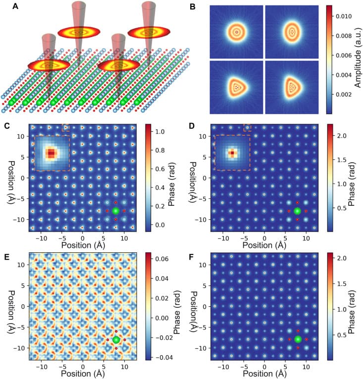
Rys. 1. Rekonstrukcja ptychograficzna na symulowanych danych z aberracjami zależnymi od pozycji. (A) Schemat skanującej sondy z aberracjami zależnymi od miejsca. (B–F) Amplitudy sond i fazy obiektu rekonstruowane metodami CPP i eLOP dla próbek 20 nm i 60 nm. Yang et al., Science Advances 12(23), 2026, DOI: 10.1126/sciadv.aec9348. Licencja: CC BY-NC 4.0.
Solution from a scientific article
In June 2026, researchers from Tsinghua University in Beijing—Wenfeng Yang, Haozhi Sha, Jizhe Cui, and Rong Yu—published inScience Advancesa work that pushes that boundary three times. The article "Imaging thick objects with deep-subangstrom resolution and deep-subpicometer precision" (DOI: 10.1126/sciadv.aec9348) presents the techniqueeLOP (ang. extended local-orbital ptychography— extended ptychography of local orbitals) combined with energy filtering of the electron beam.
Key innovation: eLOP tracks and corrects aberrationslocally— separately for each scan point. Conventional ptychographic algorithms assume that aberrations are constant or change predictably across the imaging field, which is why they fail in thicker materials where electrons scatter repeatedly. Additional energy filtering removes the signal from electrons that have lost energy in inelastic collisions with the sample - another source of noise that destroys previous reconstructions.
The effect is measurable. The authors achieved a complete ptychographic reconstructionsilicon with a thickness of 85 nm— so far beyond practical reach. The precision of determining the positions of Si atoms was0.39 picometers(standard deviation of the Si–Si distance in the crystal lattice). Limit of information obtained by the method:18 pm.
For reference: an angstrom (0.1 nm) is a conventional atomic measurement, roughly equivalent to the size of an atom. The radius of a hydrogen atom is 53 pm. The precision of 0.39 pm is more than a hundred times smaller - deep in the range calleddeep-subpicometer. The authors obtained analogous results for a 60 nm thick SrTiO₃ perovskite: precision 0.42 pm, information limit 16 pm.
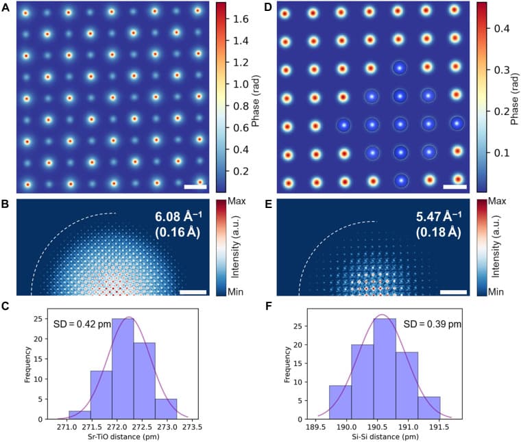
Rys. 5. Granica informacji i precyzja pozycji atomów w grubych próbkach. (A–C) SrTiO₃, 60 nm: obraz fazowy, dyfraktogram (16 pm), histogram odległości Sr–TiO (SD = 0,42 pm). (D–F) Si, 85 nm: obraz fazowy, dyfraktogram (18 pm), histogram odległości Si–Si (SD = 0,39 pm). Yang et al., Science Advances 12(23), 2026, DOI: 10.1126/sciadv.aec9348. Licencja: CC BY-NC 4.0.
What's important - and it's important to say this openly - is that work doesn't solve the problemspeed. The method is based on 4D-STEM (four-dimensional transmission electron microscopy), recording the full diffraction pattern at each scanning point. This means huge amounts of data and acquisition times measured in minutes or hours per sample. In a factory environment, where inspection must keep up with the production line, this is a barrier that the current version of the technique cannot overcome. The authors themselves indicate accelerating the acquisition and simplifying energy filtering as necessary next steps. We rate the TRL of the work as 6–7: advanced proof-of-concept on real industrial samples, but not a ready-made implementation solution.
Commercialization proposals
Despite its limitations, eLOP opens up three realistic commercialization paths over a ten-year horizon.
Licensing of the algorithm by microscope manufacturers (horizon: 3–5 years).Companies such as Carl Zeiss, JEOL and Thermo Fisher Scientific regularly update the reconstruction software of their STEM and 4D-STEM systems. The eLOP algorithm - as a module for existing computing platforms - could be licensed by Tsinghua University or a spin-off established by the authors. Barrier: validation on materials other than silicon and SrTiO₃, integration with closed software ecosystems of equipment manufacturers.
Quality controlin-linein chip factories (horizon: 4–6 years).TSMC, Samsung and Intel conduct intensive metrology programs for sub-3 nm nodes, where atomic deviations in the gate-all-around layers determine the production output. Fact: None of these entities have announced the implementation of eLOP - this is a potential assessment, not a press release. Justified speculation: as scanning rates increase by an order of magnitude - which is happening systematically in 4D-STEM thanks to the new EMPAD detectors - and the costs of energy-filtered systems drop, ptychographyin-linewill become economically viable. Barriers: pace, resistance to environmental vibrations and process certification.
Structural analysis service for the materials industry (horizon: 2-4 years).Customers from the aviation, energy and battery industries already outsource TEM analyzes to external laboratories. eLOP - offered as a high-precision 3D imaging service for thick sections - targets a niche but lucrative segment: new alloys, composite materials, crystalline phases in cell electrodes. The entry barrier is the lowest here because existing 4D-STEM laboratories can update the software without replacing the hardware.
Polish angle:Lack of identified Polish involvement - requires further investigation. The authors represent Tsinghua University; there are no Polish centers among the affiliations. Potential entry points: The Institute of Physics of the Polish Academy of Sciences and national TEM centers have infrastructure that could be used to validate eLOP on materials important for Polish industry (photovoltaics, power electronics). Justified speculation: participation in a European research consortium - e.g. at the Ernst Ruska-Centre in Jülich - would be a natural entry path for a Polish research group.
Sources
- Yang W., Sha H., Cui J., Yu R. (2026).Imaging thick objects with deep-subangstrom resolution and deep-subpicometer precision. Science Advances, 12(23). DOI: 10.1126/sciadv.aec9348 - OA version on PubMed Central: https://pmc.ncbi.nlm.nih.gov/articles/PMC13232556/
- Yang W. et al. (2025). Preprint arXiv:2502.18294. https://arxiv.org/abs/2502.18294
Comments· 1
Test